Feeds:
Posts
Comments

Archive for the ‘Tutorials’ Category

Matlab has long been an immensely convenient tool for processing and visualizing signals in a DSP system. The tool makes it very easy to simultaneously visualize a signal in multiple domains. The following is a simple demonstration of some of these signal-processing capabilities.

The Fibonacci sequence is the sequence of numbers formed when each number in the sequence is equal to the sum of the two Fibonacci numbers immediately preceding that number. The sequence is initialized by the numbers 0 and 1, and looks something like this: 0,1,1,2,3,5,8,13,21,34,55,89,144,233,377,etc. It is trivial to design a digital filter that produces the Fibonacci sequence as it’s impulse response. The impulse response of a discrete-time or digital filter is the response produced when the filter is stimulated by the Kronecker delta function:

\delta[n] = \begin{cases}                1, & n = 0 \\          	     0, & otherwise     \end{cases}

If the initial state of such a filter is such that all internal elements are at zero, the filter described by the following difference equation can produce an impulse response equal to the Fibonacci sequence. The input and output sequences are denoted x[n] and y[n], respectively.

y[n] = x[n] + y[n-1] + y[n-2]

Taking the Z-transform of this difference equation yields the following transfer function H(z) through the filter:

\begin{array}{lcl}     H(z) & = & \frac{Y(z)}{X(z)} \\          & = & \frac{1}{1 - z^{-1} - z^{-2}} \\  	& = & \frac{z^{2}}{z^{2} - z - 1}  \end{array}

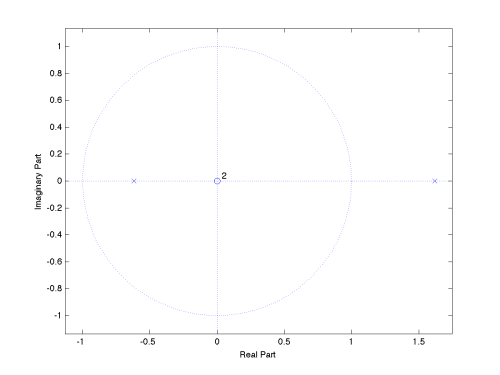
This transfer function has two zeros at the origin, and a pair of real-valued poles at z=-0.618 and z=1.618. A pole-zero plot can quickly be produced using the roots and zplane commands in Matlab:

zplane(roots([1,0,0]), roots([1,-1,-1]))

For the transfer function H(z), the coefficient matrices of the numerator and denominator polynomials in z-1 are given by B=[1] and A=[1,-1,-1], respectively. The frequency response of the filter can easily be computed using the freqz command in Matlab. In the following snippet of code, H is the complex-valued DFT and W is a vector of radian frequencies at which H has been computed. The following plot shows the magnitude of the frequency response.

% numerator polynomial
B = [1];
% denominator polynomial
A = [1,-1,-1];
% compute frequency response
[H,W] = freqz(B,A);
% plot the magnitude response (normalize W to pi)
plot(W/pi,abs(H));

The frequency response is computed along the unit circle in the Z-domain (z=ejw). Since the response is symmetric, the above plot only shows W/pi going from 0 to 1. As expected, the magnitude response shows peaks near 0 and 1, due to the relative proximity of the poles to these two points.

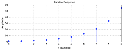
In the time-domain (or sample-domain), the response of such a system to a particular input sequence can easily be computed using the filter command in Matlab. In the following fragment of code, the above filter polynomials are used, along with initial states of zero. The input stimulus sequence x is ten samples of a Kronecker delta function, starting at n=0 and ending at n=9. The filter output y is initially 0, but then proceeds through the next ten numbers in the Fibonacci sequence.

% Kronecker delta function starting from n=0 to n=9
x = [1,zeros(1,9)];
% initial conditions of filter
init = [0,0];
% compute the filter response
y = filter(B,A,x,init);

A quicker way to compute the impulse response is through the impz command. The following line of code not only gives the first 10 values of the impulse response, it also produces a stem-line plot of the impulse response.

% compute impulse response
impz(B,A,10)

A simpler way to implement a Fibonacci sequence generator would be to discard the input x and initialize the filter to [1,0] instead of [0,0]. In any case, the Fibonacci filter example is not really practical, as the numbers increase until the internal states exceed the numerical limitations of the implemented machine. An unbounded response indicates that the filter is unstable, and this is confirmed by the location of a pole outside the unit circle in the Z-domain.

Copyright © 2012 Waqas Akram. All Rights Reserved.

Read Full Post »

During a recent interview, the great musician Neil Young expressed his desire for high-quality formats for music downloads. In terms of popular music, high-quality refers to file formats which preserve high-resolution data (e.g. 24-bit) sampled at rates much higher than necessary (e.g. 192 kHz). Whereas recording the original sources at higher sampling rates may provide some benefits with respect to the particular equipment being used, preserving these sample rates for distribution of the final mixed music makes no sense. An excellent discussion of why this format is unnecessary can be found here (xiph.org).

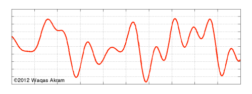
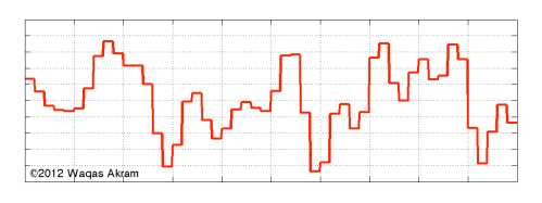
Over the years, many “audiophiles” have insisted on creating new file formats, distributing the audio files at absurd sampling rates, for the sake of “remaining faithful to the original audio waveform.” While many people know about the sampling theorem, there is a common misconception present in the minds of the lay-person when they look at the image of a sampled waveform and try to apply their intuition: they see the output of a the sampling process as a disjointed and distorted-looking stair-step response.

It has become common practice to represent the sampled waveform through an analog-to-digital converter (ADC) as a stair-step response (including on this blog). This representation is not strictly correct because it presumes that signals produced at the output of an ADC have a continuous-time representation. What actually emerges from an ADC is a signal in the discrete-time domain, where the waveform discontinuous and only exists at the sampling instants. This may seem like a trivial point, but there are ramifications for the untrained eye. When someone who is not well-versed in signal processing theory views an image showing the classic stair-step sampled waveform, their mind intuitively views this as a grossly degraded version of the original waveform. This leads to scores of “audiophiles” to incorrectly assume that an audio signal sampled at 192 kHz is inherently “more accurate” than more traditional (and sufficient) rates of 44.1 kHz (compact disc) or 48 kHz.

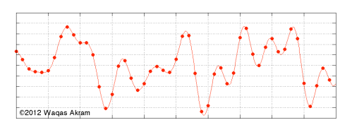
In reality, the output of an ADC looks more like a discontinuous sequence of points (“dots”) which when interpolated recreate the original signal. When such an image is shown to the human eye, the sampled waveform does not appear as distorted as the stair-step representation. The digital (discrete-time) circuitry that follows the ADC has no concept of what the signal might look like in-between the samples. The signal only exists at the active clock edges, and as long as Nyquist is satisfied the samples accurately represent the input waveform (assuming all setup-time and hold-time constraints also remain satisfied).

In order to understand how the stair-step response comes about, we need to consider the operation of a digital-to-analog converter (DAC). When converting a discrete-time signal to a continuous-time waveform, something known as a reconstruction filter is required. This reconstruction filter is specially designed to produce a continuous-time output when provided with a discrete-time input. A common type of DAC reconstruction filter is the zero-order hold, which is implemented by simply holding constant the previous sample until the next sample is encountered. The zero-order hold reconstruction filter is what leads to the aforementioned stair-step representation of the input signal. The sight of this repulsive-looking waveform leads to further questions. What do those “stair-steps” represent? Are they harmful? How do we remove these effects to recreate the original smooth signal? In order to answer these questions, we must dig deeper.

The filtering operation is basically a time-domain convolution of the input signal with the filter’s impulse response. This corresponds to a multiplication in the frequency domain. The impulse response of a zero-order hold reconstruction filter is a single square pulse, with a width equal to the sampling period. Its frequency-domain representation looks like a sinc function, which continues forever in both positive and negative frequency directions, with nulls at multiples of the sampling rate. Any discrete-time signal has a frequency-domain representation which contains an infinite number of copies of the input signal band, spaced at multiples of the sampling rate. The time-domain convolution of this signal with the reconstruction filter is equivalent to the multiplication of their frequency-domain representations.

As a result, the reconstructed signal still contains an infinite number of copies of the original waveform, albeit attenuated as we move further and further away from the origin in the frequency domain. The presence of these higher-frequency copies is what leads to the stair-step shape of the signal waveform. As long as the repeated copies can be removed without harming the primary signal band, the original signal can be perfectly reproduced without any loss. These copies need to be filtered out in order to leave us with a clean single spectral copy of the original waveform. This is usually achieved using a low-pass filter at the output. Throughout this signal-chain, there are practical issues that need to be dealt with, such as correcting the pass-band droop in both the reconstruction and the low-pass filters, as well as compensating for any phase non-linearities.

The point of all this is that what actually emerges at the output of an ADC is a series of instantaneous sample dots, floating in time and space, and ready to be consumed by the next discrete-time (digital) processing circuit. The human brain finds it much easier to spatially interpolate these points and imagine these to be a reasonably accurate representation. However, a stair-step depiction of the waveform is not only rejected by our intuition, but strictly speaking, it is also not what actually emerges from the ADC as digital samples. The stair-step waveform more closely represents an intermediate signal within a DAC that happens to use a zero-order hold reconstruction filter, and this is the wrong waveform to which the lay-person’s intuition should be applied.

Copyright © 2012 Waqas Akram. All Rights Reserved.

Read Full Post »

Non-determinism in HDLs

Digital logic can be modeled and simulated using an event-driven simulator in a hardware description language (HDL), such as Verilog or VHDL. When these models are used for synthesis into logic gates, the HDL code is necessarily restricted to a subset of the respective language, as required by the synthesis tool in use. There exist industry-established guidelines for writing synthesizable code, and every synthesis tool vendor can provide a good reference.

Unfortunately, one of the greatest challenges during integration and IP reuse of legacy Verilog code is the potential for non-deterministic behavior during execution. These issues typically arise when there is an execution race condition within the Verilog code. Although a wider discussion of the relative strengths of each language is beyond the scope of this essay, these race conditions are not possible in legacy VHDL code, due to the determinism inherently guaranteed by the language definition.

Unlike strongly-typed languages such as C or VHDL, the Verilog language was not standardized by the IEEE until after it had achieved widespread popularity. As a result, the language started off with a de facto standard as defined by the behavior of the Verilog-XL compiler/simulator (which is currently owned by Cadence). Unfortunately, flaws in this de facto language definition allowed users the latitude to create code that exhibited simulator-dependent behavior during execution.

One such example of non-deterministic behavior can occur when blocking assignments are used without care. In any HDL, there are two types of signal assignments: blocking and non-blocking. A blocking assignment is executed immediately, just as in any sequential programming language such as C. A non-blocking assignment is added to an event-queue and not executed until a subsequent iteration, in keeping with the semantics of the particular event-driven programming language being used. This behavior gets further complicated when time delays are added.

The following snippet of Verilog code (from Clifford Cummings, Nonblocking Assignments in Verilog Synthesis, Coding Styles That Kill!, SNUG-2000) illustrates an example of simulator-dependent behavior:

module fbosc1 (y1, y2, clk, rst);
    output y1, y2;
    input clk, rst;
    reg y1, y2;
    always @(posedge clk or posedge rst)
        if (rst)  y1 = 0; // reset
        else      y1 = y2;
    always @(posedge clk or posedge rst)
        if (rst)  y2 = 1; // preset
        else      y2 = y1;
endmodule // fbosc1

The Verilog standard does not require the two “always” blocks to be executed by the simulator in any particular order, and as a result, the final values of the variables y1 and y2 become dependent on the order in which the simulator decides to execute the blocks. Fortunately, this problem can be entirely avoided by using non-blocking statements instead, as shown below.

module fbosc2 (y1, y2, clk, rst);
    output y1, y2;
    input clk, rst;
    reg y1, y2;
    always @(posedge clk or posedge rst)
        if (rst)  y1 <= 0; // reset
        else      y1 <= y2;
    always @(posedge clk or posedge rst)
        if (rst)  y2 <= 1; // preset
        else      y2 <= y1;
endmodule // fbosc2

In fact, there are many published guidelines on good Verilog design practices, and these are largely followed by the design community nowadays. However, it is a significant shortcoming of a language when “best practices” are required to ensure deterministic behavior of the executed code.

This kind of behavior is avoided when using VHDL, which purposefully limits the scope of variables which can accept blocking assignments. Where Verilog uses the reg and wire transport types, VHDL uses only signal. According to the VHDL language definition, a signal can only accept non-blocking assignments, which in turn are handled via the event queue. However, blocking assignments can be made to the variable type, but by definition the scope of a variable is restricted to within a process block (a process block in VHDL is equivalent to an always block in Verilog). If it is desired that the value of a computed variable be made visible outside a process block, the value of the variable needs to first be assigned to a signal (whose scope by definition extends to the hierarchy above). As a result, the language definition preserves determinism by preventing the occurrence of race conditions created by careless use of blocking assignments.

As mentioned above, this post is not meant for passing judgement on the suitability of using either VHDL or Verilog for a particular purpose. Rather, it is intended as a warning and encouragement to heed established guidelines for achieving the best results. Nowadays, robust design methodologies require certain Verilog compiler flags and Lint options to be enabled in order to allow detection of such cases so they may be corrected before simulation. However, older code bases of unknown origin and questionable quality can still pose a potential source of problems and project delays. Seasoned industry veterans advocate the use of extensive simulation verification test suites in order to provide confidence, but a “deterministic by compilation” approach will always be preferred.

Copyright © 2008 – 2012 Waqas Akram. All Rights Reserved.

Read Full Post »

Before embarking on a new design, it is important to plan ahead and create a strategy for verifying the correct operation of that design. In the case of designing digital circuitry in a hardware description language (HDL), it is best to begin with the testbench before creating the actual design itself. In this way, as the design evolves, the testbench can be continuously modified to actively verify the incremental changes as they occur.

When designing a testbench, file input/output can be an extremely useful feature in order to read-in stimulus data from a file, and write-out results to another file. This allows one to create stimulus and verify correctness of results outside the actual language domain used for designing the block. For example, when designing a DSP system, it is common to use a high-level modeling tool such as Matlab to create and model the system. When a particular portion of the datapath is implemented in RTL, the stimulus at the input and the expected data at the output can all be written out directly from Matlab. These files can then be fed to the event-driven HDL simulation environment of the block and testbench in order to ensure direct equivalence between the two embodiments of the design.

For example, the following Matlab commands can write out the elements of a vector Vstim as single integers on each line in the text file named “teststim.txt”:

% create the vector of integers
Vstim = [5, -3, 19, 7, -13, 10];
% open the file in 'write' mode
FID = fopen('teststim.txt','w');
% write the vector to the file, one element per line
fprintf(FID,'%d\n',Vstim)
% close the file
fclose(FID)

The file “teststim.txt” should now contain the following:

5
-3
19
7
-13
10

Reading and writing files in VHDL is a fairly straight-forward process, but some details need to be settled before proceeding. There are multiple approaches to the read and write flow in a testbench: all-at-once, just-in-time, or some mixture of both. This decision can have an effect on simulation time and size, and also depends on the amount of data involved at each end.

For example, one approach might be to read-in the entire stimulus file before presenting each element to the device under test (DUT) on a clock-cycle to clock-cycle basis. Another approach might be to read-in only what is required for each cycle and waiting until the next element is actually required. Similarly at the output side, data can either be written out as it is produced by the DUT, or it can be saved until the simulation is complete, and then written out all at once. The following is a description of an example VHDL testbench which performs file I/O. It is missing a DUT, but it illustrates file I/O in VHDL.

The first thing to be declared is the testbench entity. Since the testbench is the top-level module, the entity declaration is empty. This is followed by library declarations and the definition of the testbench architecture. The internal constants and signals are described within the code comments:

-- entity declaration for testbench named "fileio"
entity fileio is
end fileio;

-- library declarations
library STD, IEEE;
-- needed for the write and read calls
use STD.textio.all;
-- needed for std_logic data types
use IEEE.std_logic_1164.all;
-- needed for calls to WRITE(LINE, std_logic)
use IEEE.std_logic_textio.all;
-- needed for calls to CONV_STD_LOGIC_VECTOR
use IEEE.std_logic_arith.all;

-- definition of architecture "BEH" for testbench "fileio"
architecture BEH of fileio is

    constant CLK_PERIOD : time := 5 ns; -- period of system clock
    constant DATA_WIDTH : integer := 6; -- width of data vector

    -- definitions of input and output file names and access types
    file INPUT_FILE     : TEXT open READ_MODE is "teststim.txt"; 
    file OUTPUT_FILE    : TEXT open WRITE_MODE is "testout.txt";
    
    signal clk_sys      : std_logic := '0'; -- system clock
    signal eof          : std_logic := '0'; -- flag end of file
    signal read_en      : std_logic := '0'; -- enable reading
    signal write_en     : std_logic := '0'; -- enable writing

    -- data vector for representing stimulus integers
    signal current_data_vec : std_logic_vector(DATA_WIDTH-1 downto 0) 
        := (others=>'0');

begin -- begin body of architecture BEH

      -- [ THIS IS WHERE ALL PROCESSES GO, AS DEFINED BELOW ]

end BEH; -- end body of architecture BEH

The system clock is defined in order to provide a cyclic reference point for all operations, including reading and writing data. There is a constant declaration for the clock period (arbitrarily defined as 5 ns in this example). The following VHDL line defines the system clock with a perfect 50% duty-cycle:

    -- create the system CLOCK
    clk_sys <= not clk_sys after CLK_PERIOD/2;

The main control process is where the testbench is controlled, and in this example, the process lacks a sensitivity list. A process without a sensitivity list simply executes code sequentially and repeats indefinitely (until the simulation is terminated). In the case of this example, the simulation is terminated using a “fake” assertion failure, in order to allow the testbench to work on arbitrarily-long stimulus files.

    -- MAIN CONTROL process
    main_control:
    process
    begin
        -- wait until the next rising clock edge
        wait until clk_sys'event and clk_sys='1';
        read_en <= '1'; -- enable reading
        -- delay writing to the output file by one clock cycle
        wait for CLK_PERIOD;
        write_en <= '1'; -- enable writing
        -- wait for the eof flag to go high
        wait until (eof='1');
        wait for CLK_PERIOD;
        -- close both files
        file_close(INPUT_FILE);
        file_close(OUTPUT_FILE);
        -- terminate the simulation
        assert false
            report "INFO: this is used to terminate the simulation"
            severity failure;
    end process main_control;

The read process is sensitive only to the system clock, responds on every rising edge of the system clock and continues to read while reading is enabled. This process keep reading until end-of-file is reached. Reading is enabled through the “read_en” signal, and end-of-file is indicated through the “eof” signal. Data is converted to a vector so the DUT can process the digital representation of the data.

    -- READ FILE process
    read_from_file:
    process (clk_sys) is
        variable tmp_line : line;
        variable tmp_int : integer;
    begin
        if (clk_sys'event and clk_sys='1' and read_en='1' 
	    and eof='0') then
            if endfile(input_file) then
                -- place the status string into a line
                write(tmp_line, string'("INFO: reached end of file"));
                -- write the line to the output
                writeline(output, tmp_line);
                -- update the flag
                eof <= '1';
            else
                -- read the next line in the file
                readline(INPUT_FILE, tmp_line);
                -- parse the line and convert data to integer
                read(tmp_line, tmp_int);
                -- convert the integer to vector and assign to a signal
                current_data_vec <= 
                    CONV_STD_LOGIC_VECTOR(tmp_int,DATA_WIDTH);
                -- maintain the flag
                eof <= '0';
            end if;
        end if;
    end process read_from_file;

The write process is sensitive only to the system clock, responds on every rising edge of the system clock and continues writing until one clock cycle after the end-of-file is reached in the stimulus file. This single-cycle delay at the end is specified in the main control process, and can be adjusted according to the desired latency through the DUT.

    -- WRITE FILE process
    write_to_file:
    process (clk_sys) is
        variable tmp_line : line;
    begin
        if (clk_sys'event and clk_sys='1' and write_en='1' 
	    and eof='0') then
            write(tmp_line, current_data_vec);
            writeline(OUTPUT_FILE, tmp_line);
        end if;
    end process write_to_file;

The above testbench can be easily be compiled and simulated using GHDL (as outlined in this post) using the following shell script:

# Compile the vhdl file
wine ghdl.exe -a --ieee=synopsys fileio.vhd
# Elaborate the testbench
wine ghdl.exe -e --ieee=synopsys fileio
# Simulate the testbench
wine ghdl.exe -r --ieee=synopsys fileio

When the simulation is run, the shell output should look something like this:

INFO: reached end of file
fileio.vhd:52:9:@42500ps:(assertion failure): INFO: this is used to terminate the simulation
C:\Program Files\Ghdl\Bin\ghdl.exe:error: assertion failed
C:\Program Files\Ghdl\Bin\ghdl.exe:error: simulation failed

The output file “testout.txt” should contain the following lines of signed integer converted to a two’s complement representation of the contents of “teststim.txt”.

000101
111101
010011
000111
110011
001010

In this example the digital data is being written directly to the output file in order to illustrate file I/O. In reality, it would be more convenient to convert the output of the DUT back to a signed integer before writing to the output file, thereby allowing Matlab to easily process and verify the output.

This type of testbench is just the first step to block-level design. The next step would be to actually design and instantiate the block (or DUT) into the testbench, taking care of any interface requirements. Throughout the design process, the testbench will have to keep up with the signalling needs of the block to be tested, as the needs arise.

Copyright © 2010-2012 Waqas Akram. All Rights Reserved.

Read Full Post »
This is a continuation of a discussion about quantization and analog-to-digital converters. In that discussion, the normalized quantization step through an N-bit ADC was denoted q, where q = 1/2N. The ADC encoder transfer function yielded a quantization error range over the interval [-q/2,+q/2].

Quantization is a highly nonlinear process. Denoting the input and output of a quantizer as u[n] and uq[n], respectively, the error from quantization uq[n]-u[n] can be re-arranged to yield the additive noise model of quantization error: uq[n]=u[n]+e, where e is the quantization error.

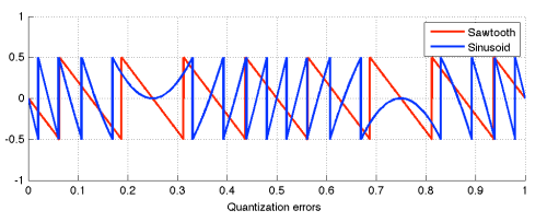
The figure below shows the quantization error for a full-scale sine wave over a single period. Also shown is the quantization error for a full-scale sawtooth ramp signal.

Although the quantization error from the sinusoid is signal-dependent and nonlinear, the commonly used additive noise model assumes a stochastic process in order to simplify the analysis. In particular, the error is treated as an independent and identically distributed (i.i.d.) random variable.

If the quantization error is modeled as a random variable with a uniform distribution, the probability density function is given by:

p(e) = \begin{cases}              0, & x \mbox{ \textless } -q/2 \\            1/q, & -q/2 \leq x \leq +q/2 \\              0, & x \mbox{ \textgreater } +q/2          \end{cases}

The root mean-square (RMS) quantization error with such a distribution can thus be derived:

\begin{array}{lcl}  e_{RMS}^2 & = & E(e^2) \\       	  & = & \int\limits_{-q/2}^{+q/2} e^2 \cdot p(e) \,d e \\       	  & = & \frac{1}{q} \int\limits_{-q/2}^{+q/2} e^2 \,d e \\       	  & = & \frac{q^2}{12} \\    e_{RMS} & = & \frac{q}{\sqrt{12}}  \end{array}

The RMS value of a full-scale sinusoid whose peak-to-peak swing has been normalized to unity is given by:

sig_{RMS} = \frac{1}{2\sqrt{2}}

The signal-to-quantization-noise ratio (SQNR) through the ADC can then be computed and expressed in decibels (dB) as:

\begin{array}{lcl}  SQNR_{sig} & = & 10log_{10} \left( \frac{sig_{RMS}}{e_{RMS}} \right)^2 \\             & = & 10log_{10} \left( \frac{1}{2\sqrt{2}} / \frac{q}{\sqrt{12}} \right)^2  \end{array}

Substituting q=1/2N gives:

\begin{array}{lcl}  SQNR_{sig} & = & 10log_{10} \left( 2^N \cdot \sqrt{3/2} \right)^2 \\             & = & 20log_{10} \left( 2^N \right) + 20log_{10} \left( \sqrt{3/2} \right) \\             & = & (6.02N + 1.76) dB  \end{array}

This is the well-known equation for SNR or dynamic range through an N-bit ADC using the additive noise model of quantization error, and in the absence of all other noise sources like thermal noise in the analog circuitry, dither and sampling jitter. Note that no over-sampling is assumed here.

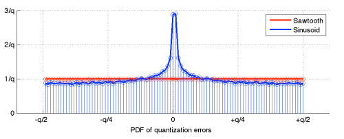
This analysis assumes that quantization errors are uniformly distributed over the quantization interval. In reality, the errors are not uniformly distributed for a sinusoidal input. For example, referring back to the time-domain quantization error from a sinusoid and a sawtooth ramp shown in the figure above, the respective error distributions are shown in the figure below.

The quantization error of the sawtooth wave appears to be uniformly distributed, but that of the sinusoid is clearly not. This is due to the signal-dependence of the sinusoid’s quantization error. Since the sawtooth actually produces uniformly distributed quantization errors, it is instructive to compute the SQNR from quantizing such a signal.

The RMS value of a full-scale sawtooth whose peak-to-peak swing has been normalized to unity is given by:

saw_{RMS} = \frac{1}{2\sqrt{3}}

Using the RMS quantization error derived above for a uniformly distributed quantization error, the SQNR of a sawtooth wave applied to an ADC can be expressed as:

\begin{array}{lcl}  SQNR_{saw} & = & 10log_{10} \left( \frac{saw_{RMS}}{e_{RMS}} \right)^2 \\             & = & 10log_{10} \left( \frac{1}{2\sqrt{3}} / \frac{q}{\sqrt{12}} \right)^2 \\             & = & 10log_{10} \left( 2^N \right)^2 \\             & = & (6.02N) dB  \end{array}

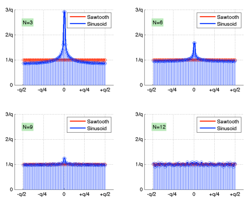
In general, the computed SQNR depends on the signal source and the model used for the quantization error. For sinusoidal inputs, the approximation of uniformly distributed quantization error improves as the ADC precision increases.

The figure below compares the error distribution of the sawtooth with that of four ADC resolutions (3 bits, 6 bits, 9 bits, and 12 bits). Clearly, the distribution approaches the quantization model of a sawtooth as the ADC resolution is increased.

Modeling the SQNR as 6dB per bit of ADC precision is a good approximation, especially as the ADC precision asymptotically increases. For many signal processing applications, the usefulness of approximating the quantization error as an i.i.d. noise source, far exceeds the inaccuracy of the model.

Copyright © 2008 – 2012 Waqas Akram. All Rights Reserved.

Read Full Post »

An Analog-to-Digital Converter (ADC) does exactly what the name implies: it converts an analog electrical signal to a digital representation. Specifically, the analog signal is a continuous-time continuous-amplitude signal, and the digital signal representation produced by the typical ADC is a sequence of discrete-time discrete-amplitude samples. The process of conversion from a high-resolution signal to a low-resolution signal is also known as quantization.

The two main types of ADCs are oversampling converters and Nyquist-rate converters, and there are several architectures for these. In most cases, there is some form of uniform quantization being performed on a high-resolution signal, in order to represent it in terms of a finite set of quantization levels. The error that results from quantization is referred to as quantization error. The spectral representation of random quantization error is known as quantization noise.

An ADC requires a clock signal to synchronize the instances when the analog signal is sampled. The clock frequency is referred to as the sampling rate, i.e. the rate at which samples are taken, and can be denoted fs. It is important that the clock have little or no clock jitter, which creates uncertainty in the sampling instant, and hence increases the quantization error.

An ADC also typically requires a reference voltage, denoted by VREF, which determines the valid voltage range over which the analog input signal can be converted. The input range of an ADC that only operates on positive voltages would go from zero volts, or circuit ground, to VREF. If the analog signal takes on values outside this voltage range, a well-designed input circuit will non-catastrophically limit the ADC to either minimum or maximum voltage, depending on the input signal. As expected, this would produce either a minimum or maximum digital value at the output.

The most common representation used for the digital samples produced by an ADC is a string of binary digits (or bits), where 00..0 represents the smallest analog input, and 11..1 represents the largest. These are sometimes referred to as ADC output codes. An N-bit binary number can represent at most 2N unique levels, and therefore, an N-bit ADC can produce 2N unique codes.

The quantization step or width of each ADC code can be denoted q, where q = VREF/2N. The nominal ADC code width is expected to be equal to a single LSB (least-significant bit), which is the right-most bit in a binary word representation. When the code width is normalized to VREF, q = 1/2N.

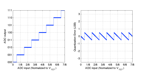
In the figure above, an example of a 3-bit ADC encoder transfer function is shown on the left, relating the digital output to the analog input. The encoder transfer function is arranged so that any input signal less than q/2 produces the smallest digital code, 000, input signals between q/2 and 3q/2 produce the next digital code 001, and so on. Alternate arrangements are possible, depending on the specific application requirements of the ADC.

The quantization error resulting from using this encoder transfer function is shown in the figure above on the right, and in this case, it takes values over the interval [-q/2,+q/2]. This assumes that the ADC input is appropriately limited and the digital output code is saturated when the input signal goes outside the operating range of the ADC.

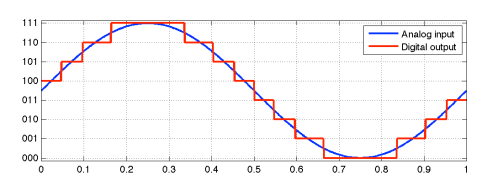
The figure below shows the result when a full-scale sine wave is provided at the input to an ADC with this encoder transfer function.

It should be apparent that quantization is a highly non-linear process, and this makes it very difficult to perform an exact analysis of an otherwise linear system. In order to use classical linear analysis, it is necessary to derive a suitable linearized model of the quantizer, and this will be covered in a future post.

Copyright © 2008 – 2012 Waqas Akram. All Rights Reserved.

Read Full Post »
The use of the decibel scale is ubiquitous in electronic systems. For example, the dynamic range through a system is measured by the signal-to-noise ratio in decibels, or dB. When working in the lab, or viewing the output of any measurement device, it is useful know how to make quick mental conversions between the linear and dB scales.

The amplitude or power of a signal is typically quantified relative to a fixed reference. A full-scale signal has a ratio of 1:1, and is expressed as 20.log(1/1) = 0 dB. Remember that multiplication (division) in the linear domain is equivalent to addition (subtraction) in the log domain. One needs to only remember a few values in order to compute most conversions:

  1. A ten-fold (10x) increase or decrease in linear signal amplitude results in a +20 dB or -20 dB change on the decibel scale, respectively.
  2. A doubling or halving (2x or ½x) of linear signal amplitude results in [approximately] a +6 dB or -6 dB change on the decibel scale, respectively.
  3. A tripling (3x) of linear signal amplitude can be approximated by using 3 ≈ √10. The square-root is equivalent to a power of half, and in the log domain, this simply halves the dB value. This results in ½ x 20 dB = 10 dB.

Using these basic rules, it is easy to quickly compute the linear ratios corresponding the dB value. Note that in the list above, the 3x ↔ 10 dB conversion is the greatest source of error in the final approximation.

Some examples:

  • Convert 54 dB to the linear scale: note that 54 dB = (60 – 6) dB, which is equivalent to 1000 x ½ = 500 in the linear domain (this is a good approximation to the actual value of 501.2)
  • Convert 7x to the dB scale: note that 7 = √49 ≈ √50 = √(100 x ½), which is equivalent to ½ x (40 – 6) = 17 dB (the answer should be 16.9)
  • Convert 30 dB to the linear scale: note that 30 dB = (20 + 10) dB, which is equivalent to (10 x 3) = 30 in the linear domain (the answer should be 31.6). Alternatively, we can use 30 dB = (40 – 10) dB, which converts to (100 ÷ 3) = 33.3 (the magnitude of the approximation error is about the same as that of the first answer)

In the computerized world of today (or when no one brings a calculator to the lab), these mental shortcuts can be very useful as a quick sanity check.

Copyright © 2008 – 2012 Waqas Akram. All Rights Reserved.

Read Full Post »